No products
Prices are tax excluded
Product successfully added to your shopping cart
There are 0 items in your cart. There is 1 item in your cart.


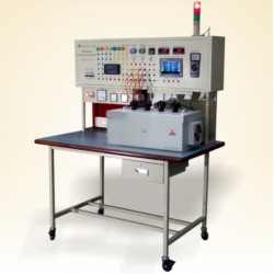
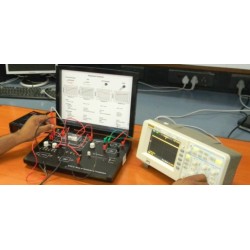
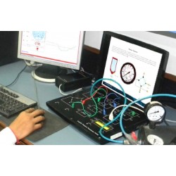
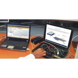
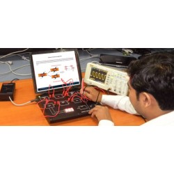
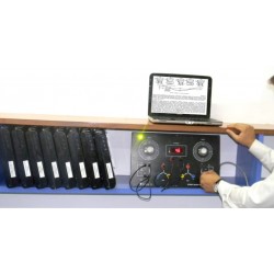
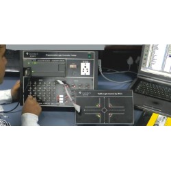
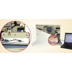
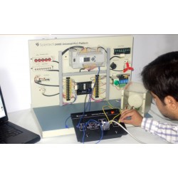
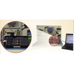
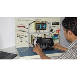
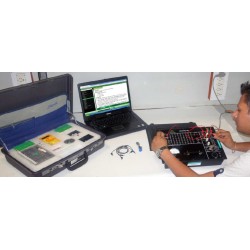
Nvis 1801 PCB Design & Development Lab
Nvis1801
New
Nvis 1801 PCB Lab is a complete solution for designing Printed Circuit Boards. This solution includes all necessary machines and chemicals which are required in the PCB development process.
- Consulta este producto
- Remove this product from my favorite's list.
- Add this product to my list of favorites.
| Category | PCB |
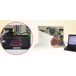
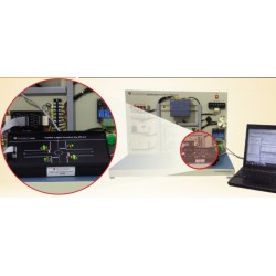
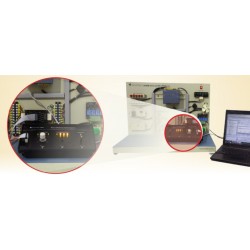
In this Lab, PCB fabrication is carried out using the Screen Printing Method. The PCB Layout generated from CAD Tools is used as fabrication input for the PCB manufacturing. The PCB Shearing Machine is used for cutting PCBs as per the PCB layout size. The PCB Screen Printing Unit helps to coat the printing silk screen with light sensitive material. The PCB layout and light sensitive coated screen is placed in the UV Exposure Unit for exposing. The UV exposure and development process transfers the image from PCB layout to printing screen. After exposure the screen is developed with the help of washing gun provided. The PCB Screen Printing Unit is used again for transferring the screen image on the PCB laminate. The PCB Curing Machine is used as heating oven. The PCB Etching Machine is used for removing unused copper from the PCB. The Drill Machine is used for making holes in the PCB.
30 other products in the same category:
-
Scientech24...
-
Scientech24...
-
Scientech24...
-
Scientech23...
-
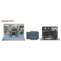
ScientechIT...
-
Scientech24...
-
Scientech24...
-
Scientech24...
-
Scientech24...
-
Scientech24...
-
Scientech24...
-
Scientech23...
-
Scientech23...
-
Scientech23...
-
Scientech23...
-
Scientech23...
-
Scientech23...
-
Scientech23...
-
Scientech23...
-
Scientech23...
-
Scientech24...
-
Scientech24...
-
Scientech24...
-
Scientech24...
-
Scientech24...
-
Scientech24...
-
Scientech24...
-
Scientech24...
-
Scientech24...
-
Nvis 6000...
550,00 €